

 |
CD54HC299F3A IC Chip Shift Shift Register 1 Element 8 Bit 20-CDIP
Product Details:
| Place of Origin: | original |
| Brand Name: | original |
| Certification: | original |
| Model Number: | CD54HC299F3A |
Payment & Shipping Terms:
| Minimum Order Quantity: | 1 |
|---|---|
| Price: | negotiation |
| Packaging Details: | carton box |
| Delivery Time: | 1-3working days |
| Payment Terms: | T/T |
| Supply Ability: | 100,000 |
|
Detail Information |
|||
| Logic Type: | Inverter | Number Of Circuits: | 6 |
|---|---|---|---|
| Number Of Inputs: | 6 | Features Schmitt: | Trigger |
| Voltage - Supply: | 2V ~ 3.6V | Current - Quiescent (Max): | 1 µA |
| Current - Output High, Low: | 24mA, 24mA | Input Logic Level - High: | 1.3V ~ 2V |
| Max Propagation Delay @ V, Max CL: | 6.2ns @ 3.3V, 50pF | Operating Temperature: | -55°C ~ 125°C |
| High Light: | CD54HC299F3A IC Chip,IC Chip Shift Shift Register,1 Element 8 Bit 20-CDIP |
||
Product Description
CD54HC299F3A IC chip Shift Shift Register 1 Element 8 Bit 20-CDIP
HIGH SPEED CMOS LOGIC 8-BIT UNIV
Specifications of CD54HC299F3A
| TYPE | DESCRIPTION |
| Category | Integrated Circuits (ICs) |
| Logic | |
| Shift Registers | |
| Mfr | Texas Instruments |
| Series | 54HC |
| Package | Tube |
| Product Status | Active |
| Logic Type | Shift Register |
| Output Type | Tri-State |
| Number of Elements | 1 |
| Number of Bits per Element | 8 |
| Function | Universal |
| Voltage - Supply | 2V ~ 6V |
| Operating Temperature | -55°C ~ 125°C (TA) |
| Mounting Type | Through Hole |
| Package / Case | 20-CDIP (0.300", 7.62mm) |
| Supplier Device Package | 20-CDIP |
Features of CD54HC299F3A
• Buffered Inputs
• Four Operating Modes: Shift Left, Shift Right, Load and Store
• Can be Cascaded for N-Bit Word Lengths
• I/O0 - I/O7 Bus Drive Capability and Three-State for Bus Oriented Applications
• Typical fMAX = 50MHz at VCC = 5V, CL = 15pF, TA = 25oC
• Fanout (Over Temperature Range)
- Standard Outputs . . . . . . . . . . . . . . . 10 LSTTL Loads
- Bus Driver Outputs . . . . . . . . . . . . . 15 LSTTL Loads
• Wide Operating Temperature Range . . . -55oC to 125oC
• Balanced Propagation Delay and Transition Times
• Significant Power Reduction Compared to LSTTL Logic ICs
• HC Types
- 2V to 6V Operation
- High Noise Immunity: NIL = 30%, NIH = 30% of VCC at VCC = 5V
• HCT Types
- 4.5V to 5.5V Operation
- Direct LSTTL Input Logic Compatibility,
VIL= 0.8V (Max), VIH = 2V (Min)
- CMOS Input Compatibility, Il ≤ 1µA at VOL, VOH
Descriptions of CD54HC299F3A
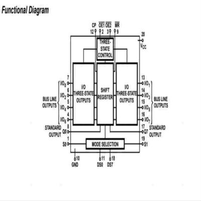
The ’HC259 and ’HCT299 are 8-bit shift/storage registers with three-state bus interface capability. The register has four
synchronous-operating modes controlled by the two select inputs as shown in the mode select (S0, S1) table. The mode
select, the serial data (DS0, DS7) and the parallel data (I/O0- I/O7) respond only to the low-to-high transition of the clock
(CP) pulse. S0, S1 and data inputs must be stable one setup time prior to the clock positive transition.
Environmental & Export Classifications of CD54HC299F3A
| ATTRIBUTE | DESCRIPTION |
| RoHS Status | ROHS3 Compliant |
| Moisture Sensitivity Level (MSL) | Not Applicable |
![]()