

 |
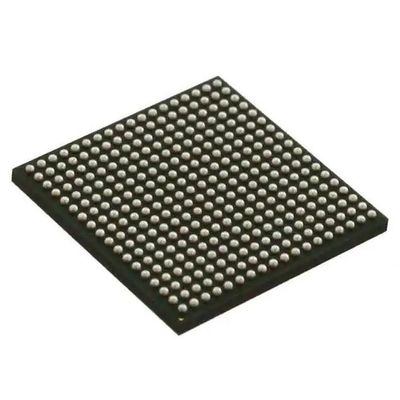
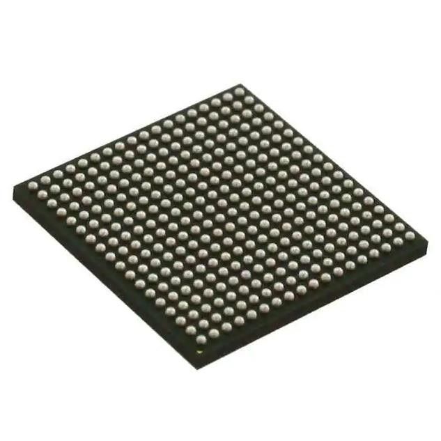
AM3357BZCZA30 IC Chip Mpu Sitara 300MHZ 324 NFBGA ADE Chip
Product Details:
| Place of Origin: | original |
| Brand Name: | original |
| Certification: | original |
| Model Number: | AM3357BZCZA30 |
Payment & Shipping Terms:
| Minimum Order Quantity: | 1 |
|---|---|
| Price: | negotiation |
| Packaging Details: | carton box |
| Delivery Time: | 1-3working days |
| Payment Terms: | T/T, L/C |
| Supply Ability: | 100,000 |
|
Detail Information |
|||
| Mfr: | Texas Instruments | Series: | Sitara™ |
|---|---|---|---|
| Package: | Tray | Product Status: | Active |
| Core Processor: | ARM® Cortex®-A8 | Number Of Cores/Bus Width: | 1 Core, 32-Bit |
| Speed: | 300MHz | ||
| High Light: | AM3357BZCZA30 IC Chip,Mpu Sitara 300MHZ 324NFBGA,324 FBGA ADE Chip |
||
Product Description
AM3357BZCZA30 Integrated Circuit IC Chip Mpu Sitara 300mhz 324nfbga
ARM® Cortex®-A8 Microprocessor IC Sitara™ 1 Core, 32-Bit 300MHz 324-NFBGA (15x15)
Specifications of AM3357BZCZA30
| TYPE | DESCRIPTION |
| Category | Integrated Circuits (ICs) |
| Embedded | |
| Microprocessors | |
| Mfr | Texas Instruments |
| Series | Sitara™ |
| Package | Tray |
| Product Status | Active |
| Core Processor | ARM® Cortex®-A8 |
| Number of Cores/Bus Width | 1 Core, 32-Bit |
| Speed | 300MHz |
| Co-Processors/DSP | Multimedia; NEON™ SIMD |
| RAM Controllers | LPDDR, DDR2, DDR3, DDR3L |
| Graphics Acceleration | Yes |
| Display & Interface Controllers | LCD, Touchscreen |
| Ethernet | 10/100/1000Mbps (2) |
| SATA | - |
| USB | USB 2.0 + PHY (2) |
| Voltage - I/O | 1.8V, 3.3V |
| Operating Temperature | -40°C ~ 105°C (TJ) |
| Security Features | Cryptography, Random Number Generator |
| Mounting Type | Surface Mount |
| Package / Case | 324-LFBGA |
| Supplier Device Package | 324-NFBGA (15x15) |
| Additional Interfaces | CAN, I²C, McASP, McSPI, MMC/SD/SDIO, UART |
| Base Product Number | AM3357 |
Features of AM3357BZCZA30
• Up to 1-GHz Sitara™ ARM® Cortex®
-A8 32‑BitRISC Processor
– NEON™ SIMD Coprocessor
– 32KB of L1 Instruction and 32KB of Data CacheWith Single-Error Detection (Parity)
– 256KB of L2 Cache With Error Correcting Code(ECC)
– 176KB of On-Chip Boot ROM
– 64KB of Dedicated RAM
– Emulation and Debug - JTAG
– Interrupt Controller (up to 128 InterruptRequests)
• On-Chip Memory (Shared L3 RAM)
– 64KB of General-Purpose On-Chip MemoryController (OCMC) RAM
– Accessible to All Masters
– Supports Retention for Fast Wakeup
• External Memory Interfaces (EMIF)
– mDDR(LPDDR), DDR2, DDR3, DDR3LController:
– mDDR: 200-MHz Clock (400-MHz Data Rate)
– DDR2: 266-MHz Clock (532-MHz Data Rate)
– DDR3: 400-MHz Clock (800-MHz Data Rate)
– DDR3L: 400-MHz Clock (800-MHz DataRate)
– 16-Bit Data Bus
– 1GB of Total Addressable Space
– Supports One x16 or Two x8 Memory DeviceConfigurations
– General-Purpose Memory Controller (GPMC)
– Flexible 8-Bit and 16-Bit AsynchronousMemory Interface With up to Seven ChipSelects (NAND, NOR, Muxed-NOR, SRAM)
– Uses BCH Code to Support 4-, 8-, or 16-BitECC
– Uses Hamming Code to Support 1-Bit ECC
– Error Locator Module (ELM)
– Used in Conjunction With the GPMC toLocate Addresses of Data Errors fromSyndrome Polynomials Generated Using aBCH Algorithm
– Supports 4-, 8-, and 16-Bit per 512-ByteBlock Error Location Based on BCHAlgorithms
• Programmable Real-Time Unit Subsystem andIndustrial Communication Subsystem (PRU-ICSS)
– Supports Protocols such as EtherCAT®,PROFIBUS, PROFINET, EtherNet/IP™, and More
– Two Programmable Real-Time Units (PRUs)
– 32-Bit Load/Store RISC Processor Capable of Running at 200 MHz
– 8KB of Instruction RAM With Single-Error Detection (Parity)
– 8KB of Data RAM With Single-Error Detection (Parity)
– Single-Cycle 32-Bit Multiplier With 64-Bit Accumulator
– Enhanced GPIO Module Provides ShiftIn/Out Support and Parallel Latch on External Signal
– 12KB of Shared RAM With Single-Error Detection (Parity)
– Three 120-Byte Register Banks Accessible by Each PRU
– Interrupt Controller (INTC) for Handling System Input Events
– Local Interconnect Bus for Connecting Internal and External Masters to the Resources Inside the PRU-ICSS
– Peripherals Inside the PRU-ICSS:
– One UART Port With Flow Control Pins, Supports up to 12 Mbps
– One Enhanced Capture (eCAP) Module
– Two MII Ethernet Ports that Support Industrial Ethernet, such as EtherCAT
– One MDIO Port
• Power, Reset, and Clock Management (PRCM) Module
– Controls the Entry and Exit of Stand-By and Deep-Sleep Modes
– Responsible for Sleep Sequencing, Power Domain Switch-Off Sequencing, Wake-Up Sequencing, and Power Domain Switch-On Sequencing
– Clocks
– Integrated 15- to 35-MHz High-Frequency Oscillator Used to Generate a Reference Clock for Various System and Peripheral Clocks
– Supports Individual Clock Enable and Disable Control for Subsystems and Peripherals to Facilitate Reduced Power Consumption
– Five ADPLLs to Generate System Clocks
(MPU Subsystem, DDR Interface, USB and Peripherals [MMC and SD, UART, SPI, I 2C], L3, L4, Ethernet, GFX [SGX530], LCD Pixel Clock)
Applications of AM3357BZCZA30
• Gaming Peripherals
• Home and Industrial Automation
• Consumer Medical Appliances
• Printers
• Smart Toll Systems
• Connected Vending Machines
• Weighing Scales
• Educational Consoles
• Advanced Toys
Environmental & Export Classifications of AM3357BZCZA30
| ATTRIBUTE | DESCRIPTION |
| RoHS Status | ROHS3 Compliant |
| Moisture Sensitivity Level (MSL) | 3 (168 Hours) |
| REACH Status | REACH Unaffected |
| ECCN | 5A992C |
| HTSUS | 8542.31.0001 |
![]()
Want to Know more details about this product