


 |
MILITARY Programmable Logic Chips 4CH 2 INPUT 3V TO 1 CD4001BF3A
Product Details:
| Place of Origin: | original |
| Brand Name: | original |
| Certification: | original |
| Model Number: | CD4001BF3A |
Payment & Shipping Terms:
| Minimum Order Quantity: | 1 |
|---|---|
| Price: | negotiation |
| Packaging Details: | carton box |
| Delivery Time: | 1-3working days |
| Payment Terms: | T/T |
| Supply Ability: | 100,000 |
|
Detail Information |
|||
| Model: | JM38510/50404BRA | Package: | Bulk |
|---|---|---|---|
| Mfg: | TI | Temperature: | -55°C ~ 125°C |
| Product Status: | Active | ||
| High Light: | MILITARY Programmable Logic Chips,4CH Programmable Logic Chips,CD4001BF3A |
||
Product Description
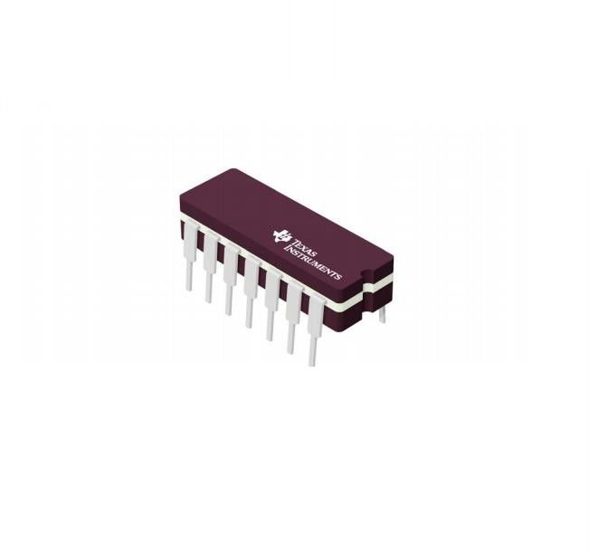
CD4001BF3A MILITARY Integrated Circuit IC Chip Logic 4-CH, 2-INPUT 3-V TO 1
NOR Gate IC 4 Channel 14-CDIP
Specifications of CD4001BF3A
| TYPE | DESCRIPTION |
| Category | Integrated Circuits (ICs) |
| Logic | |
| Gates and Inverters | |
| Mfr | Texas Instruments |
| Series | - |
| Package | Tube |
| Product Status | Active |
| Logic Type | NOR Gate |
| Number of Circuits | 4 |
| Number of Inputs | 2 |
| Features | - |
| Voltage - Supply | 3V ~ 18V |
| Current - Quiescent (Max) | 5 µA |
| Current - Output High, Low | 6.8mA, 6.8mA |
| Input Logic Level - Low | 1.5V ~ 4V |
| Input Logic Level - High | 3.5V ~ 11V |
| Max Propagation Delay @ V, Max CL | 90ns @ 15V, 50pF |
| Operating Temperature | -55°C ~ 125°C |
| Mounting Type | Through Hole |
| Supplier Device Package | 14-CDIP |
| Package / Case | 14-CDIP (0.300", 7.62mm) |
Features of CD4001BF3A
■ Propagation delay time=60 ns(typ.)at CL=50pF,VDD=10V
■ Buffered inputs and outputs
■ Standardized sy mmetrical output characteristics
■ 100% testedformaximumquiescentcurrentat201 5-V.10-V,and 15-V parametric ratings
■ Maximum input current of 1μA at 18V over full package-temperature range;100 nA at 18 V and 25°c
#Noise margin(over full package temperature range):
1Vat VDD=5V 2Vat VDD=10V 2.5VatVDD-15V
■ Meets all requirements of JEDEC Tentative Standard No.13B,"Standard Specltications forDescriptionof“B”SeriesCMOSDevices”
MAXIMUM RATINGS,Absolute-Maximum Values of CD4001BF3A
DC SUPPLY-VOLTAGE RANGE.(VDD)
Voltages refarancad to Vss Terminal):-0.5V to+20V
NPUTvoLTAGE RANGE,ALL INPUTS:-0.5V to VDD +05V
DCINPUTCuARENT,AY ONEINPUT: ±10mA
POWER DISSIPATION PER PACKAGE(PD)
ForTA=-559Clo+100°C,500mW
ForTA=+100C lo125°C, Drnte Lineartys 12mwW/C lo 200mw
DEVICE DISSIPATION PER OUTPUT TRANSISTOR
FORTA=FULLPACKAGE-TEMPERATURERANGE(ALL Package Typee): 100mW
LEAD TEMPERATUAE(DURING SOLDERING):
At distance 1/16 ±1/32 inch(1.59±0.79mm)fromcase for 10s max +265°C
Environmental & Export Classifications of CD4001BF3A
| ATTRIBUTE | DESCRIPTION |
| RoHS Status | ROHS3 Compliant |
| Moisture Sensitivity Level (MSL) | Not Applicable |
| ECCN | EAR99 |
| HTSUS | 8542.39.0001 |
![]()