


 |
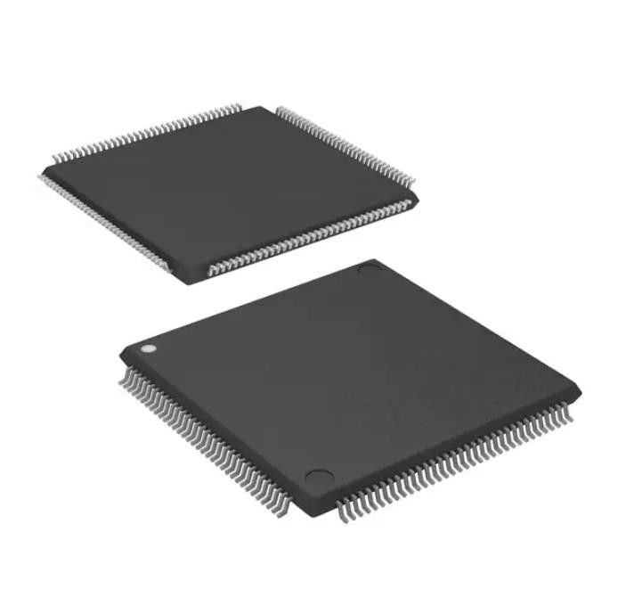
LCMXO2-1200HC-4TG144C General Purpose Relays Ic Fpga 107 I/O 144tqfp
Product Details:
| Place of Origin: | original |
| Brand Name: | original |
| Certification: | original |
| Model Number: | LCMXO2-1200HC-4TG144C |
Payment & Shipping Terms:
| Minimum Order Quantity: | 1 |
|---|---|
| Price: | negotiation |
| Packaging Details: | carton box |
| Delivery Time: | 1-3working days |
| Payment Terms: | T/T, L/C |
| Supply Ability: | 100,000 |
|
Detail Information |
|||
| Package: | Tray | Product Status: | Active |
|---|---|---|---|
| Digi-Key Programmable: | Not Verified | Number Of LABs/CLBs: | 160 |
| Number Of Logic Elements/Cells: | 1280USART | Total RAM Bits: | 65536 |
| Number Of I/O: | 107 | Voltage - Supply: | 2.375V ~ 3.465V |
Product Description
LCMXO2-1200HC-4TG144C General Purpose Relays Ic Fpga 107 I/O 144tqfp
MachXO2 Field Programmable Gate Array (FPGA) IC 107 65536 1280 144-LQFP
Specifications of LCMXO2-1200HC-4TG144C
| TYPE | DESCRIPTION |
| Category | Integrated Circuits (ICs) |
| Embedded | |
| FPGAs (Field Programmable Gate Array) | |
| Mfr | Lattice Semiconductor Corporation |
| Series | MachXO2 |
| Package | Tray |
| Product Status | Active |
| Digi-Key Programmable | Not Verified |
| Number of LABs/CLBs | 160 |
| Number of Logic Elements/Cells | 1280 |
| Total RAM Bits | 65536 |
| Number of I/O | 107 |
| Voltage - Supply | 2.375V ~ 3.465V |
| Mounting Type | Surface Mount |
| Operating Temperature | 0°C ~ 85°C (TJ) |
| Package / Case | 144-LQFP |
| Supplier Device Package | 144-TQFP (20x20) |
| Base Product Number | LCMXO2-1200 |
Features of LCMXO2-1200HC-4TG144C
Flexible Logic Architecture
• Six devices with 256 to 6864 LUT4s and 18 to 334 I/Os
Ultra Low Power Devices
• Advanced 65 nm low power process
• As low as 22 µW standby power
• Programmable low swing differential I/Os
• Stand-by mode and other power saving options
Embedded and Distributed Memory
• Up to 240 kbits sysMEM™ Embedded Block RAM
• Up to 54 kbits Distributed RAM
• Dedicated FIFO control logic
On-Chip User Flash Memory
• Up to 256 kbits of User Flash Memory
• 100,000 write cycles
• Accessible through WISHBONE, SPI, I2 C and JTAG interfaces
• Can be used as soft processor PROM or as Flash memory
Pre-Engineered Source Synchronous I/O
• DDR registers in I/O cells
• Dedicated gearing logic
• 7:1 Gearing for Display I/Os
• Generic DDR, DDRX2, DDRX4
• Dedicated DDR/DDR2/LPDDR memory with DQS support
High Performance, Flexible I/O Buffer
• Programmable sysIO™ buffer supports wide
range of interfaces:
– LVCMOS 3.3/2.5/1.8/1.5/1.2
– LVTTL
– PCI
– LVDS, Bus-LVDS, MLVDS, RSDS, LVPECL
– SSTL 25/18
– HSTL 18
– Schmitt trigger inputs, up to 0.5 V hysteresis
• I/Os support hot socketing
• On-chip differential termination
• Programmable pull-up or pull-down mode
Flexible On-Chip Clocking
• Eight primary clocks
• Up to two edge clocks for high-speed I/O interfaces (top and bottom sides only)
• Up to two analog PLLs per device with fractional-n frequency synthesis
– Wide input frequency range (7 MHz to 400 MHz)
Non-volatile, Infinitely Reconfigurable
• Instant-on – powers up in microseconds
• Single-chip, secure solution
• Programmable through JTAG, SPI or I2 C
• Supports background programming of non-volatile memory
• Optional dual boot with external SPI memory
TransFR™ Reconfiguration
• In-field logic update while system operates
Enhanced System Level Support
• On-chip hardened functions: SPI, I2 C, timer/ counter
• On-chip oscillator with 5.5% accuracy
• Unique TraceID for system tracking
• One Time Programmable (OTP) mode
• Single power supply with extended operating range
• IEEE Standard 1149.1 boundary scan
• IEEE 1532 compliant in-system programming
Broad Range of Package Options
• TQFP, WLCSP, ucBGA, csBGA, caBGA, ftBGA, fpBGA, QFN package options
• Small footprint package options
– As small as 2.5 mm x 2.5 mm
• Density migration supported
• Advanced halogen-free packaging
Slices of LCMXO2-1200HC-4TG144C
Slices 0-3 contain two LUT4s feeding two registers. Slices 0-2 can be configured as distributed memory. Table 2-1 shows the capability of the slices in PFU blocks along with the operation modes they enable. In addition, each PFU contains logic that allows the LUTs to be combined to perform functions such as LUT5, LUT6, LUT7 and LUT8. The control logic performs set/reset functions (programmable as synchronous/ asynchronous), clock select, chipselect and wider RAM/ROM functions.
Environmental & Export Classifications of LCMXO2-1200HC-4TG144C
| ATTRIBUTE | DESCRIPTION |
| RoHS Status | ROHS3 Compliant |
| Moisture Sensitivity Level (MSL) | 3 (168 Hours) |
| REACH Status | REACH Unaffected |
| ECCN | EAR99 |
| HTSUS | 8542.39.0001 |
Want to Know more details about this product