


 |
EP2C50F484C7N General Purpose Relays Ic Fpga 294 I/O 484fbga
Product Details:
| Place of Origin: | original |
| Brand Name: | original |
| Certification: | original |
| Model Number: | EP2C50F484C7N |
Payment & Shipping Terms:
| Minimum Order Quantity: | 1 |
|---|---|
| Price: | negotiation |
| Packaging Details: | carton box |
| Delivery Time: | 1-3working days |
| Payment Terms: | T/T, L/C |
| Supply Ability: | 100,000 |
|
Detail Information |
|||
| Package: | Tray | Product Status: | Active |
|---|---|---|---|
| Digi-Key Programmable: | Not Verified | Number Of LABs/CLBs: | 3158 |
| Number Of Logic Elements/Cells: | 50528 | Total RAM Bits: | 594432 |
| Number Of I/O: | 294 | Voltage - Supply: | 1.15V ~ 1.25V |
Product Description
EP2C50F484C7N General Purpose Relays Ic Fpga 294 I/O 484fbga
Cyclone® II Field Programmable Gate Array (FPGA) IC 294 594432 50528 484-BGA
Specifications of EP2C50F484C7N
| TYPE | DESCRIPTION |
| Category | Integrated Circuits (ICs) |
| Embedded | |
| FPGAs (Field Programmable Gate Array) | |
| Mfr | Intel |
| Series | Cyclone® II |
| Package | Tray |
| Product Status | Active |
| Digi-Key Programmable | Not Verified |
| Number of LABs/CLBs | 3158 |
| Number of Logic Elements/Cells | 50528 |
| Total RAM Bits | 594432 |
| Number of I/O | 294 |
| Voltage - Supply | 1.15V ~ 1.25V |
| Mounting Type | Surface Mount |
| Operating Temperature | 0°C ~ 85°C (TJ) |
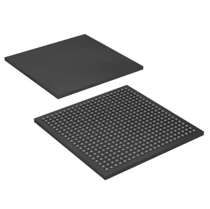
| Package / Case | 484-BGA |
| Supplier Device Package | 484-FBGA (23x23) |
| Base Product Number | EP2C50 |
Features of EP2C50F484C7N
■ High-density architecture with 4,608 to 68,416 LEs
● M4K embedded memory blocks
● Up to 1.1 Mbits of RAM available without reducing available logic
● 4,096 memory bits per block (4,608 bits per block including 512 parity bits)
● Variable port configurations of ×1, ×2, ×4, ×8, ×9, ×16, ×18, ×32, and ×36
● True dual-port (one read and one write, two reads, or two writes) operation for ×1, ×2, ×4, ×8, ×9, ×16, and ×18 modes
● Byte enables for data input masking during writes
● Up to 260-MHz operation
■ Embedded multipliers
● Up to 150 18- × 18-bit multipliers are each configurable as two independent 9- × 9-bit multipliers with up to 250-MHzperformance
● Optional input and output registers
■ Advanced I/O support
● High-speed differential I/O standard support, including LVDS, RSDS, mini-LVDS, LVPECL, differential HSTL, and differential SSTL
● Single-ended I/O standard support, including 2.5-V and 1.8-V, SSTL class I and II, 1.8-V and 1.5-V HSTL class I and II, 3.3-V PCI and PCI-X 1.0, 3.3-, 2.5-, 1.8-, and 1.5-V LVCMOS, and 3.3-, 2.5-, and 1.8-V LVTTL
● Peripheral Component Interconnect Special Interest Group (PCI SIG) PCI Local Bus Specification, Revision 3.0 compliance for 3.3-V operation at 33 or 66 MHz for 32- or 64-bit interfaces
● PCI Express with an external TI PHY and an Altera PCI Express ×1 Megacore® function
● 133-MHz PCI-X 1.0 specification compatibility
● High-speed external memory support, including DDR, DDR2, and SDR SDRAM, and QDRII SRAM supported by drop in Altera IP MegaCore functions for ease of use
● Three dedicated registers per I/O element (IOE): one input register, one output register, and one output-enable register
● Programmable bus-hold feature
● Programmable output drive strength feature
● Programmable delays from the pin to the IOE or logic array
● I/O bank grouping for unique VCCIO and/or VREF bank settings
● MultiVolt™ I/O standard support for 1.5-, 1.8-, 2.5-, and 3.3-interfaces
● Hot-socketing operation support
● Tri-state with weak pull-up on I/O pins before and during configuration
● Programmable open-drain outputs
● Series on-chip termination support
VCCA & GND of EP2C50F484C7N
■ Use separate VCCA power planes
■ Use a partitioned VCCA island within the VCCINT plane
■ Use thick VCCA traces
Environmental & Export Classifications of EP2C50F484C7N
| ATTRIBUTE | DESCRIPTION |
| RoHS Status | RoHS Compliant |
| Moisture Sensitivity Level (MSL) | 3 (168 Hours) |
| REACH Status | REACH Unaffected |
| ECCN | 3A991D |
| HTSUS | 8542.39.0001 |
Want to Know more details about this product