


 |
CDCE72010RGCT Clock Synchronizer Fanout Jitter Cleaner IC 1.5GHz 1 64-VFQFN
Product Details:
| Place of Origin: | original |
| Brand Name: | original |
| Certification: | original |
| Model Number: | CDCE72010RGCT |
Payment & Shipping Terms:
| Minimum Order Quantity: | 1 |
|---|---|
| Price: | negotiation |
| Packaging Details: | carton box |
| Delivery Time: | 3-5ddays |
| Payment Terms: | T/T |
| Supply Ability: | 1000 |
|
Detail Information |
|||
| Type: | Clock Synchronizer, Fanout (Distribution), Jitter Cleaner | PLL: | Yes |
|---|---|---|---|
| Input: | LVCMOS, LVDS, LVPECL | Output: | LVCMOS, LVDS, LVPECL |
| Number Of Circuits: | 1 | Ratio - Input:Output: | 3:20 |
| Voltage - Supply: | 3V ~ 3.6V | Frequency - Max: | 1.5GHz |
Product Description
CDCE72010RGCT Clock Synchronizer Fanout Jitter Cleaner IC 1.5GHz 1 64-VFQFN
Specifications of CDCE72010RGCT
| TYPE | DESCRIPTION |
| Category | Integrated Circuits (ICs) |
| Clock/Timing | |
| Clock Generators, PLLs, Frequency Synthesizers | |
| Mfr | Texas Instruments |
| Series | - |
| Package | Tape & Reel (TR) |
| Cut Tape (CT) | |
| Product Status | Active |
| Type | Clock Synchronizer, Fanout (Distribution), Jitter Cleaner |
| PLL | Yes |
| Input | LVCMOS, LVDS, LVPECL |
| Output | LVCMOS, LVDS, LVPECL |
| Number of Circuits | 1 |
| Ratio - Input:Output | 3:20 |
| Differential - Input:Output | Yes/Yes |
| Frequency - Max | 1.5GHz |
| Divider/Multiplier | Yes/No |
| Voltage - Supply | 3V ~ 3.6V |
| Operating Temperature | -40°C ~ 85°C |
| Mounting Type | Surface Mount |
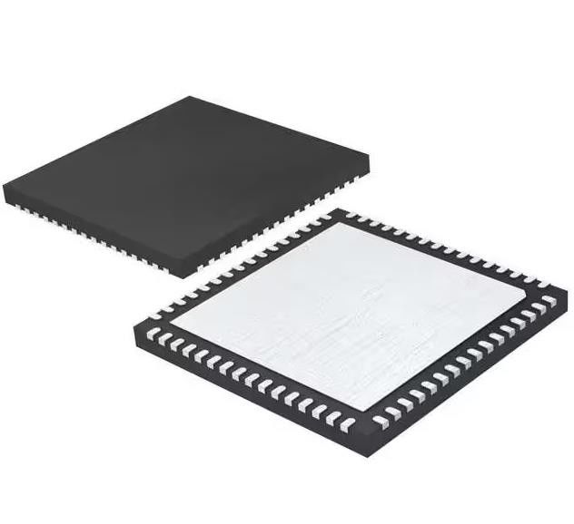
| Package / Case | 64-VFQFN Exposed Pad |
| Supplier Device Package | 64-VQFN (9x9) |
| Base Product Number | CDCE72010 |
Features of CDCE72010RGCT
* High Performance LVPECL, LVDS, LVCMOSPLL Clock Synchronizer
* Two Reference Clock Inputs (Primary andSecondary Clock) for Redundancy Supportwith Manual or Automatic Selection
* Accepts Two Differential Input (LVPECL orLVDS) References up to 500MHz (or TwoLVCMOS Inputs up to 250MHz) as PLLReference
* VCXO IN Clock is Synchronized to One of TwoReference Clocks
* VCXO IN Frequencies up to 1.5GHz (LVPECL)800MHz for LvDS and 250MHz for LVCMOSLevel Signaling
* Outputs Can be a Combination of LVPECLLVDS, and LVCMoS (Up to 10 DifferentialLVPECL or LVDS Outputs or up to 20 LVCMOSOutputs), Output 9 can be Converted to anAuxiliary Input as a 2nd VC(X)0.
Applications of CDCE72010RGCT
• Low Jitter Clock Driver for High-End Telecom and Wireless Applications
• High Precision Test Equipment
Environmental & Export Classifications of CDCE72010RGCT
| ATTRIBUTE | DESCRIPTION |
| RoHS Status | ROHS3 Compliant |
| Moisture Sensitivity Level (MSL) | 3 (168 Hours) |
| REACH Status | REACH Unaffected |
| ECCN | EAR99 |
| HTSUS | 8542.39.0001 |
![]()